
Install Steam
login
|
language
简体中文 (Simplified Chinese)
繁體中文 (Traditional Chinese)
日本語 (Japanese)
한국어 (Korean)
ไทย (Thai)
Български (Bulgarian)
Čeština (Czech)
Dansk (Danish)
Deutsch (German)
Español - España (Spanish - Spain)
Español - Latinoamérica (Spanish - Latin America)
Ελληνικά (Greek)
Français (French)
Italiano (Italian)
Bahasa Indonesia (Indonesian)
Magyar (Hungarian)
Nederlands (Dutch)
Norsk (Norwegian)
Polski (Polish)
Português (Portuguese - Portugal)
Português - Brasil (Portuguese - Brazil)
Română (Romanian)
Русский (Russian)
Suomi (Finnish)
Svenska (Swedish)
Türkçe (Turkish)
Tiếng Việt (Vietnamese)
Українська (Ukrainian)
Report a translation problem


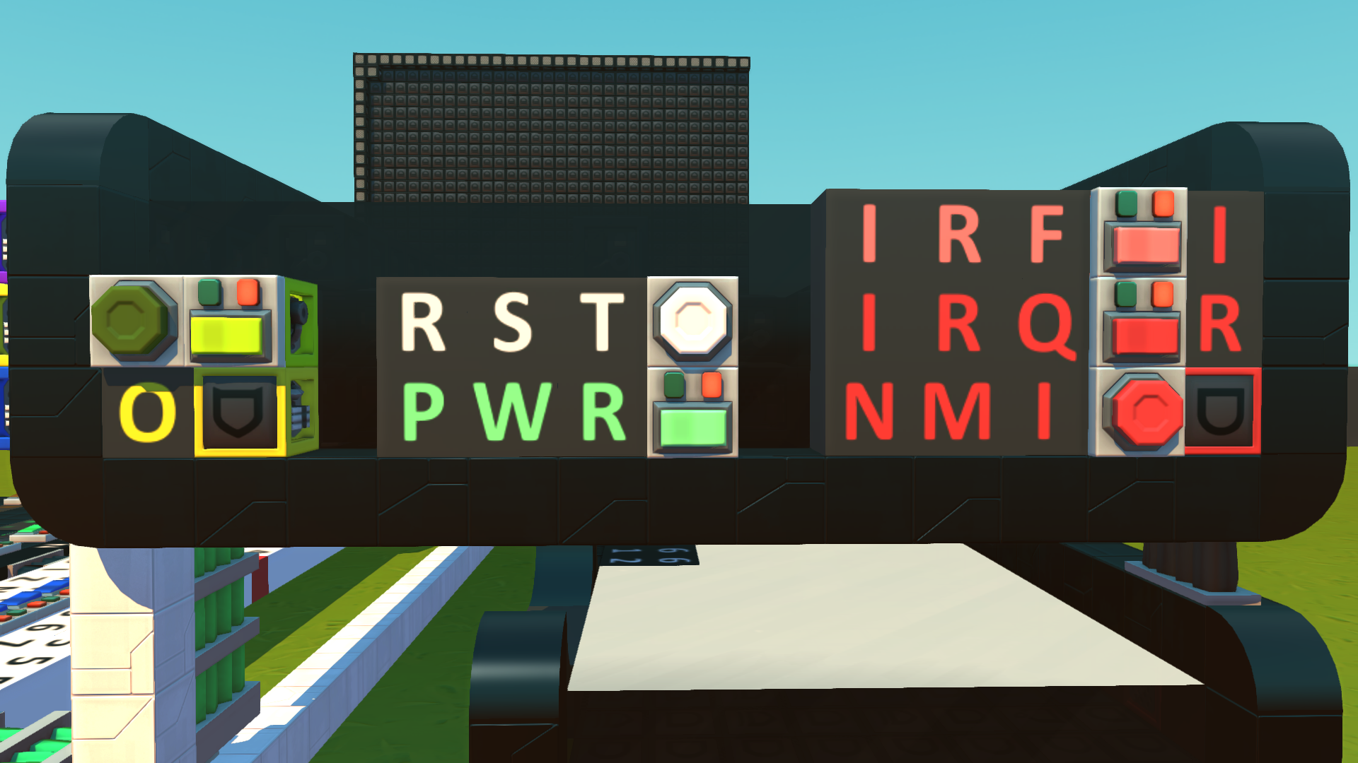
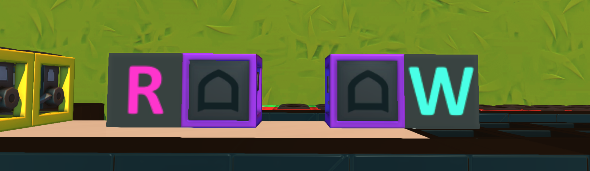
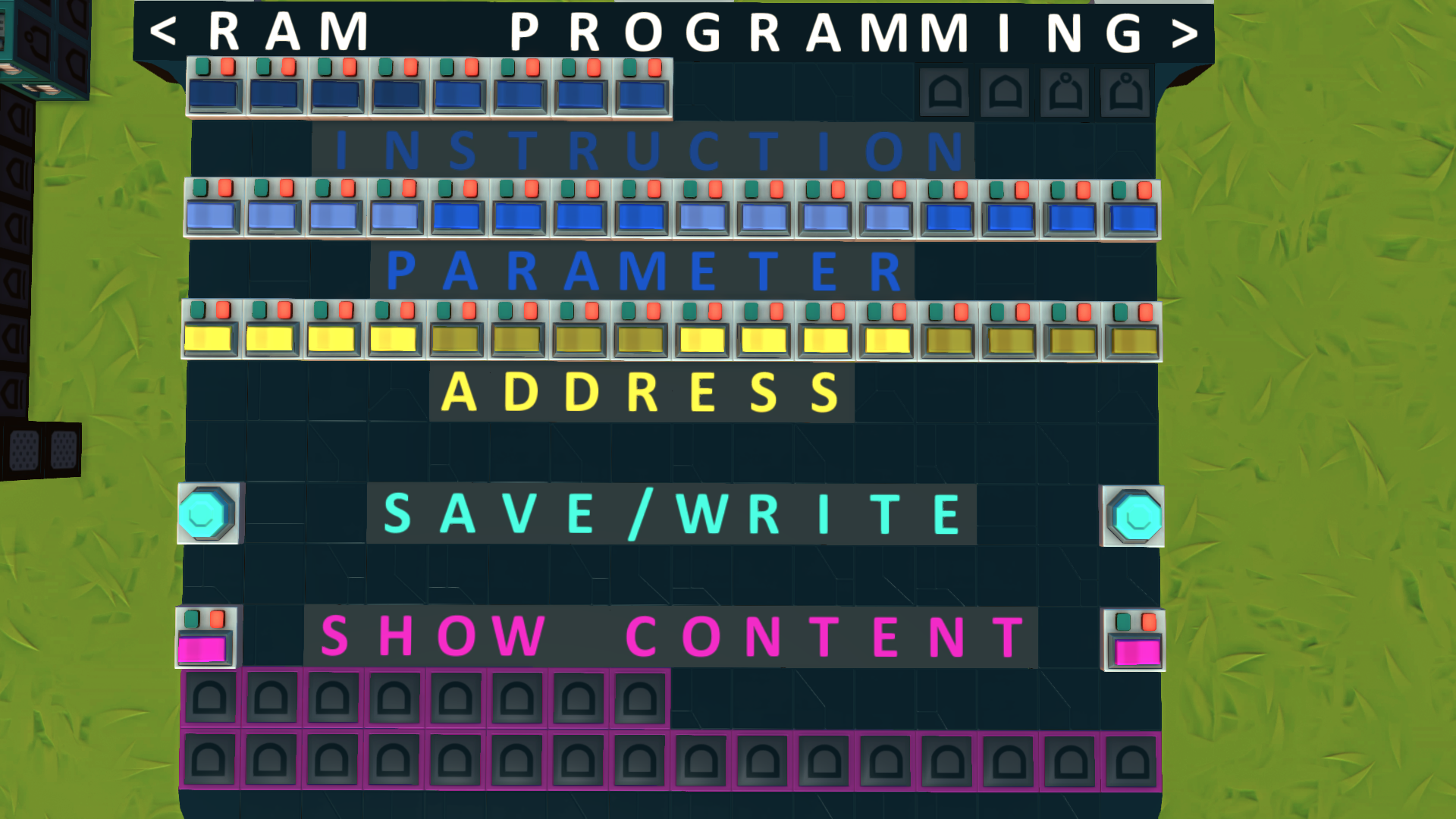
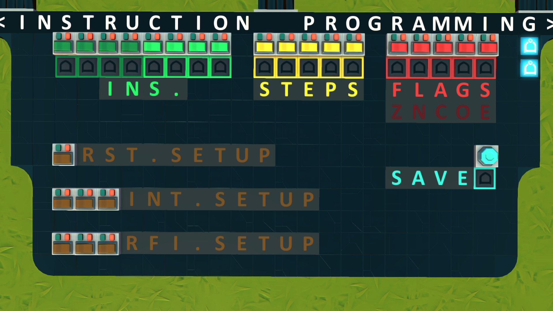
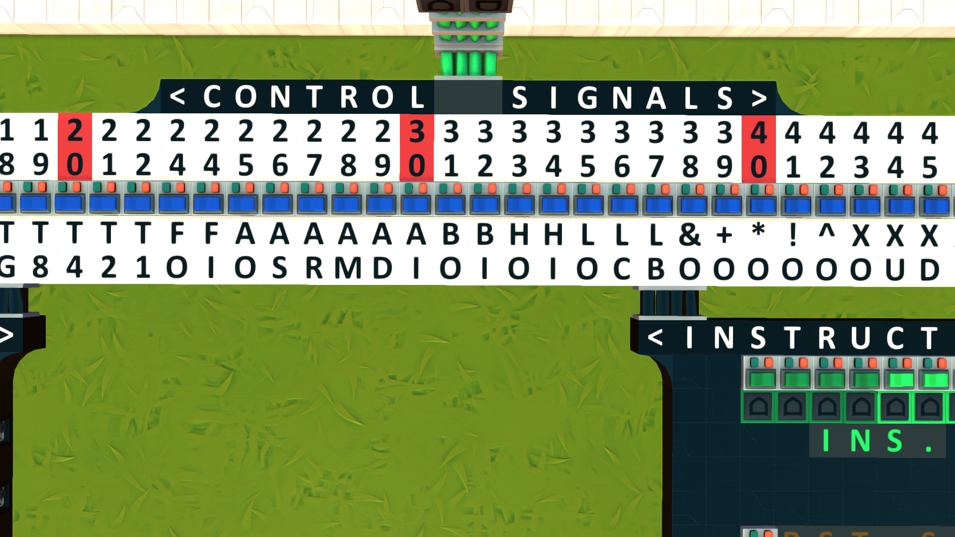


what even? XD